

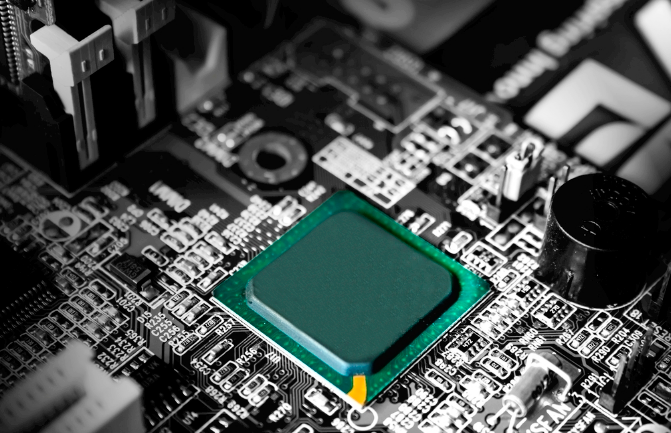
PCBA research and development
PCBA scheme design, the main enterprise engineering R&D team transforms customer ideas into feasible specific schemes, optimizes the schemes,
manufactures products, and finally converts customer ideas into physical products. The design process is as follows:
PCBA research and development
Product design: According to the customer's product design ideas, functional requirements and appearance requirements, give design plans and
documents.
Material selection: After deciding on the product design plan, select the appropriate electronic components according to the customer's cost budget,
functional specification, etc.
Structural design: PCB structural design, production of PCB proofing documents, optimization of circuits and layout of electrical components according
to customer assembly requirements. Carry out DFM analysis to identify defects in PCBA design schemes and improve the yield rate of PCBA production.
Sample manufacturing: mount finished products, deliver samples, and debug samples later.
Mass production: optimize the design and realize mass production.
PCBA design and processing requires not only a professional engineer design team, but also a complete placement production line. TOPWELLTECH has
more than 10 years of product customization experience. Welcome customers to inquiry!